2. How Nand Devices are programmed on Xeltek programmer
1)NAND FLASH的特点。
1) An introduction to Nand flash
A. NAND FLASH同NOR FLASH相比,NANDFLASH有着容量大、价格低等优势.
A. Compared with NOR FLASH, Nand flash devices have the advantages of large capacity with lower cost.
B.由于NAND生产工艺的原因,出厂芯片中会随机出现坏块。坏块在出厂时已经被初始化,并在特殊区域中标记为不可用,在使用过程中如果出现坏块,也需要进行标记.
B. Since the manufacturing method, te NAND flash may include invalid blocks when they are first shipped. Bad blocks have been initialized before shipping and marked in the specific area. New bad blocks can be generated during usage so the system will have to identify these blocks.
C. NAND FLASH更易出现位反转的现象,如果位反转出现在关键文件上,会导致系统挂机。所以在使用NAND FLASH的同时,建议使用ECC/EDC算法确保可靠性.
C. Bit inverse is easier to be found in Nand flash. If bit inverse happens in the important file, it will cause system shut-down. Therefore, ECC/EDC algorithms are suggested to use to keep reliability when programming Nand Flash.
2)NAND FLASH的坏块处理 NAND FLASH的坏块处理方式有很多,用户可以根据自己的需要选择那一种方法,或者按照自己的要求向我们公司定做。目前我们公司比较成熟、已经被使用验证过的5~6种,下面主要对最常见的三种模式进行一下说明:
2) How to handle the bad blocks
There are many methods to handle the bad blocks. The customer can choose one method according to their own requirements or request Xeltek to customize the algorithms for their own solutions. Currently, we have 5 to 6 methods to handle the bad blocks.Three common methods are introduced here.
A. 直接跳过(Skip Bad Block)
.gif)
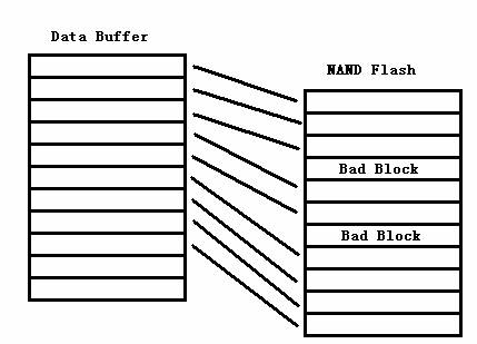
这种处理方法是最为简单,也是最常见的方法。即读取辨认坏块标志后,如果此为坏块的话,将内容写入到下一个好块中。如果是读操作的话,不处理当前坏块,跳到下一个好块进行读(如图2)。如果使用这种方式,客户需要关注图(1)中的UBA start block、Size of UBA blocks ( RBA start block、Size of RBA blocks是针对Reserved block的。Boot start block、Size of Boot blocks是检查启动代码区有没有坏块使用的)。UBA start block表示程序文件从第几block开始进行烧录,默认是从0000开始。Size of UBA blocks表示程序文件要烧录多少个block。
The skip bad block method is the simplest and most common method. This method is very straightforward. It is to just skip over the bad blocks and place the data in the good blocks. When reading a chip, the program just skip over the bad blocks and read the data in the next good blocks. Using this method, the customer needs to check User Block Area (UBA) start block、Size of UBA blocks in the figure 1. The Reserved Block Area (RBA) start block and the size of RBA blocks are used for reserved block method. Boot start block and Size of Boot blocks are used to check if there are bad blocks used in boot area. UBA start block shows the staring address to program the chip. The default address is 0000. The size of UBA blocks is the number of blocks to be programmed.
例如:程序的文件为19M,从第0个block开始烧录,目标芯片为K9F1208U0B,每个block大小为16K(大页模式为128K),则要烧写的block=19*1024/16=1216=0x4C0,为安全起见,建议留一点余量,加上0x10个block。所以UBA start block填0000, Size of UBA blocks填0x4D0.
For example, the file size is 19M and programming starts from the first block. The target chip is K9F1208U0B. Each block is 16K (Large mode is 128K). The blocks for programming = 19*1024/16=1216=0x4C0. It is suggested to add 0x10 block to make sure to have enough space. Therefore, UBA start block is 0000 and Size of UBA blocks is 0x4D0.
B. 保留替代(Reserved)
B. Reserved Block
使用这种方式编程时,将生成一个存储地址替代表。即当用户程序区出现坏块的时候,编程器软件会在Reserved区找一个好块替代它,并最终生成一张替代表,放在一个区域保留。在读写操作时,遇到坏块就读一下替代表,再读替代块的内容,这样的好处是让系统在逻辑上感觉存储器依然是连续的区域。
In this method, a mapping table will be generated. When a bad block is identified, the software will reserve a good block to replace it and creating a mapping table saved in a reserved area. When a bad block is detected during reading a chip, software will read the mapping table and then read the replaced block. The advantage is the storage area is logically continuous.
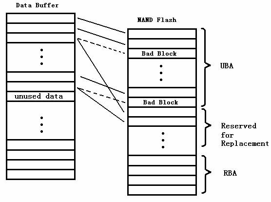
如图3,UBA区是存放用户代码区的,RBA区是存放替代表的,Reserved for Replacement区是存放用户代码区出现坏块替代的内容的。
如图1中填写的话。UBA区是从0000~0EFF, RBA区是从0F80~0F8F, Reserved for Replacement区是从0F00~0F7F。Reserved for Replacement区是UBA与RBA中间的一段区域。
In figure 3, UBA is User Block Area. RBA is Reserved Block Area.Reserved for Replacement
Between the starting address of UBA and RBA, there are some reserved for replacement blocks used for replacing the bad blocks.
C.分区模式(Partition)
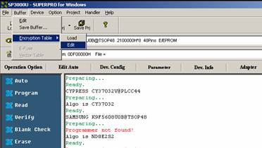
分区模式是由一张分区表对NAND进行定位烧写的。在烧录准备前,先要装载或编辑一张分区表如图4&图5。
C. Partition
Partition is used to Nand programming based on a partition table. A partition table is loaded and edited before programming, shown in Figure 4 and Figure 5.
(图4)Figure 4
在分区表中,每16个字节代表一个分区,16个字节中的第1~4个字节表示该分区的起始块地址,第5~8个字节表示该分区的结束块地址,第9~12个字节表示该分区实际使用到的块大小,第13~16个字节为保留字节。当遍历到分区的起始块地址为FF FF FF FF时,遍历结束。当在烧录过程中遇到坏块时,按Skip Bad Block处理。故如图5所示,该目标芯片要烧录三个分区,第一个分区的起始块地址为0000,结束块地址为007F,实际使用的块大小为0001。
In the partition table, every 16-byte represents a partition, in which the bytes from 1st to 4th represents the starting block address, the bytes from the 5th to 8th represent the ending block address, the bytes form 9th to 12th represent the block size actually used, the bytes from 13th to 16th is the conserved bytes. The address searching will end until the starting address is FF FF FF FF. The skip bad block method is used during programming. For example, there are three partitions need to be programmed for this chip. The starting address and the ending address for the first
partition are 0000 and 007F.The actual block size is 0001.
3)NAND FLASH的Spare Area的使用。
关于Spare Area的使用在如图1中的Spare Area(ECC)中设置。如果您要烧录的文件中已经包含了Spare Area的信息,请选择Used选项;如果您要烧录的文件中没有包含Spare Area的信息并且Spare Area也不需要任何处理,请选择Reserved, ECC disabled;如果您选择了Reserved, ECC enabled,表示您使用编程器计算出来的ECC算法。我们编程器默认使用的为512B ECC算法,以如下表的结构分布的。
0~4th |
5th |
6~8th |
9~12th |
13~15th |
Reserved |
Bad Mark |
ECC0 |
ECC1 |
ECC2 |
Reserved |
ECC0 |
ECC1 |
ECC2 |
如果您希望XELTEK编程器为您计算Spare区要存放的数据,请将您的要求详细告诉我们.
3) Spare Area in NAND FLASH
About the usage of Spare Area, we need to set the Spare Area (ECC) in Figure 1. If the file for programming includes Spare Area information, please select “Used”. If there is no Spare Area information in the file for programming, please select “Reserved, ECC disabled”. If you select “Reserved ,ECC enabled”, you will use the ECC algorithm generated by the software. The default algorithm used by our programmer is 512B ECC algorithm. Table 1 shows the format.
Table 1
0~4th |
5th |
6~8th |
9~12th |
13~15th |
Reserved |
Bad Mark |
ECC0 |
ECC1 |
ECC2 |
Reserved |
ECC0 |
ECC1 |
ECC2 |
If you want XELTEK programmer to calculate the data for saving to Spare Area, please tell us the requirement in details.
4)关于Boot Block Check。
一般情况,程序的Boot区是不允许有坏块的,所以在使用NAND芯片时,检查一下boot区的坏块情况是有必要的,如果您的Boot区安排在第0个block,一般情况下不需要检察坏块,因为芯片在出厂时已经保证了第0个block不是坏块。检查的设置如图1,其中Boot start block表示启动代码区的起始块,Size of Boot blocks启动代码区的大小。如果设置Size of Boot blocks为All blocks(全部块大小),就可以检查出整个NAND的坏块情况。
4) Generally, bad blocks are not allowed to reside in boot area. Therefore it is necessary to check if there are bad blocks in boot area when programming NAND chips. If your boot area is in the first block, there is no need to check the bad block since most NAND manufacturers guarantee that the first block is good. Figure 1 show the boot area configuration. Boot start block shows the starting address of boot area. Size of Boot blocks is the size of boot area. Size of Boot blocks is set to be the size of all blocks in order to check all bad blocks of the Nand chip.
5)坏块标志位。
一般情况,大页模式的坏块标志位为每个block的第2048个字节,小页模式的坏块标志位为每个block的第517个字节,所以在烧录文件中坏块标志位的内容必须为FF,如果您的程序中使用了非标准处理方法,请联系我们,我们会按您的要求提供算法。
5) Bad block mark
In general, the bad block mark for large page mode is in the 2948 byte of every block and in the 517 byte of every block. Therefore, the content of the bad block mark in the programming file is FF. If you didn’t use standard processing method in your file, please contact us. We will customize the algorithm according to your requirements.
6)关于新烧录模式、文件系统和Spare区特殊信息等的开发支持
如果您有如下的开发需求,请给我们提供详细的说明,我们会努力满足您的需求。
A.新的坏块处理方法。
B.非标准的坏块标志位。
C.使用ECC512B&ECC256W以外的ECC算法。
D. Spare区存放扇区,块使用次数,程序文件的其他信息。
E.需要文件系统(FFS)的支持。
....................................
6) About support for new programming mode, file system and specific information of spare area
Please provide the detail description about your development requirements. We will try to fulfill your requirements.
- New bad block processing method.
- Non standard bad block mark.
- Using ECC algorithm except ECC512B & ECC256W.
- Saving sector, block usage time, programming file or other information to Spare Area.
- Need FFS support.
3.NAND FLASH烧录常见问题解答
3. NAND FLASH programming FAQ
1) Config Error错误,不允许继续操作。
出现这样的情况是由于器件配置字(Dev.Config)中的参数设置不当。正确的设置应该是这样的:UBA start block应该是小于All Blocks,Size of UBA blocks应该小于或者等于All Blocks减去UBA start block。Boot start block应该是小于All Blocks,Size of Boot blocks小于或者等于All Block减去UBA start block。
如果在Reserved模式下面,UBA start block应该是小于RBA start block ,Size of UBA blocks 也应该是小于RBA start block减去UBA start block,RBA start block应该大于UBA start block加Size of UBA blocks、并且小于All Blocks,Size of RBA blocks应该小于All Blocks减去RBA start block。
1) Config Error, not allow to continue operation
The problem happens because the variables in Dev. Config is not set properly.
Correct setting is: UBA start block < All Blocks,
Size of UBA blocks <= (All Blocks - UBA start block)
Boot start block < All Blocks
Size of Boot blocks <= (All Block - UBA start block)
2)编程中提示Good blocks not enough.
这是由于要烧录的数据超过了芯片好块的大小,所以设置器件配置字(Dev.Config)还应该结合芯片的实际情况,如果检查出芯片中有16个坏块,那实际的好块(ALL Blocks)应该相应减去0x10.
有时在读写母片时也会出现这样的情况,而且检查坏块多少时发现有很多的坏块。这是因为母片中的坏块标志位被转移到其他的地方。默认的坏块标志位被写成有效的数据。
2) Programming message problem about “Good blocks not enough”
This problem happens because the programming file is larger than the size of all good blocks in the chip. Therefore, setting the value in Dev. Config should consider the actual size of the chip. If 16 bad blocks is detected in the chip, the actual good block size should be equal to (All Blocks – 0x10).
The similar problem could happen while reading and programming the master chip. More bad blocks will properly be detected, since the bad block mark of the mother chip is moved to other places. The default bad block mark is written as effective data.